

Modeling the Local Annealing of Color Centers in Diamond and Silicon Carbide via Nanosecond-Pulsed Lasers
General Overview

Quantum computers are poised to lead a revolution in computing capabilities, offering performance that far exceeds what is physically possible with classical computers. Instead of relying on classical bits, the ones and zeroes that form binary, quantum computers utilize qubits, which can exploit the physics of individual atoms and their interactions to conduct calculations with staggering power. Current quantum computer infrastructure relies on either individually trapped atoms in a vacuum or superconducting circuits. A third basis for qubits involves color centers, which are point defects in crystal structures with fascinating optical and electronic properties. They fluoresce brightly at well-characterized wavelengths, and since this emission is often dependent on the state of the electrons (excited and spin-up or spin-down), it is very easy to obtain a readout of the current state. Coupled with easy manipulation of spin states and long-lived coherence, this makes color centers an incredibly promising avenue for constructing logical qubits.
Two well-studied color centers are the silicon vacancy in silicon carbide and the nitrogen-vacancy center in diamond (NV center). While their synthesis is readily achievable, localization is needed on the order of 1 micrometer to 10 nanometers in order to be fully realized in computing frameworks and sensing applications. Laser processing of the host materials, diamond and silicon carbide, has proven useful in the vacancy generation step, but work must be done on understanding how to localize the annealing step, which heals crystal lattice damage and finalizes color center formation.
To achieve this, transient thermal simulations were conducted in MATLAB and Python to determine temperature diffusion profiles, diffusion timescales, and maximum temperatures reached. The laser in question produces a 1 nanosecond pulse with the beam focused at the surface of the diamond or silicon carbide sample, and to model the light-matter interaction, various heating profiles were examined.
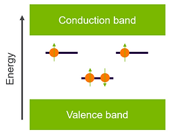
Left: Diagram of the electronic structure of a color center in a wide bandgap material, such as diamond. The energy levels of the electrons associated with the color center defect lie within the bandgap and are effectively isolated from the bulk material, serving as a model of an isolated atom.
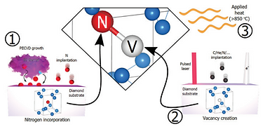
Right: A flowchart indicating the various synthesis methods used to generate NV centers. Nitrogen is introduced into the crystal during chemical vapor deposition, vacancies are generated through laser processing or other methods, and the crystal is annealed to let the vacancies and nitrogen fuse. Smith, et al. Nanophotonics, 8, 1890 (2019)
A variety of issues arose during the investigation, including long processing times, data overflows, unrealistically high temperatures, and difficulties in modelling the heat source. The pyPDE package, a partial differential equation solver in Python that includes support for the heat equation, was expanded to permit the modelling of time-dependent external heat sources, and results were cross-checked with output from the MATLAB Thermal Toolbox. While MATLAB remained slow in its calculations, pyPDE was accelerated using the Numba package, reducing simulation times from 30 minutes to 5 seconds. Unfortunately, pyPDE cannot account for temperature-dependent properties, and given that anticipated temperatures range from 5 K to 1200 K, the changes in thermal conductivity and specific heat capacity cannot be ignored. MATLAB can accurately model such temperature-dependent properties at the expense of long processing times, and limited computing resources hindered the length of time that could be modeled.
Ultimately, final simulation results were presented to the QIS research group at Argonne National Laboratory within the Material Sciences Division (MSD). Qualitative knowledge of diffusion profiles has been obtained, with diffusion happening on the order of tens of nanoseconds to microseconds in thermally conductive diamond/silicon carbide. It has been recognized that the light-matter interaction in highly transparent wide-band-gap materials is poorly captured in the literature, and experiments are underway to directly measure the temperatures achieved at peak laser intensity. While limited in scope, these simulations are important in advancing towards an all-optical manufacturing process for color centers, which can rapidly scale and permit for use in quantum computing and sensing.